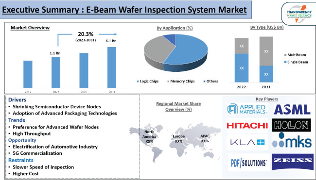
Global E-beam Wafer Inspection System Market: Snapshot
Wafer inspection systems are required for timely detection of physical and technological defects present within wafers. Currently, both e-beam and optical technologies are used in the detection of defects in wafers. With the application of e-beams manufacturers of compact devices are able to timely detect faults in wafers, thus saving the additional expenditure, which otherwise they would incur on re-inspection. The technology therefore ensures long-term usage of wafers across various industrial verticals. This has emerged as a key reason, positively impacting the overall trajectory of the global e-beam wafer inspection system market.
Increasing applications of thin wafers in manufacturing small or miniaturized devices used in micro-electro mechanical systems, laptops, and smartphones among others have bolstered the demand for e-beam wafer inspection system. Also the market is forecast to gain from the persistently rising activities in the semiconductor industry. These industrial activities will continue rising over the forecast period, delivering the e-beam wafer inspection system market with ample opportunities to gain from.
Free Customization as per your requirement, Buy Now
Spurred by the aforementioned factors, the global e-beam wafer inspection system market is forecast to exhibit a CAGR of 17.5% between 2015 and 2025. Rising at this rate, the market will reach US$1.06 bn by the end of 2025, from US$248.3 million in 2016.

Detection Imaging to Remain Dominant Segment Based on Application
Based on type, the global e-beam wafer inspection system market is segmented into less than 1 nm, 1 to 10 nm and more than 10 nm inspection resolution system. In 2016, e-beam wafer inspection system market was dominated by more than 10 nm wafer inspection systems, followed by the other two segments. However, during the forecast period the less than 1 nm segment will showcase a higher CAGR.
On the basis of application, the global e-beam wafer inspection system market has been segmented into defect imaging, lithographic qualification, bare wafer OQC/IQC, wafer dispositioning, reticle quality inspection, and inspector recipe optimization. Of these, defect imaging formed the largest application segment with a share of 38.5% in the market in 2016. It is expected to remain dominant through the course of the forecast period. Besides this, inspector recipe optimization followed by bare wafer OQC/IQC have emerged as the application segments exhibiting strong prospects for the market.
Get More Press Releases by TMR: https://www.prnewswire.com/news-releases/long-term-health-hazards-loss-of-natural-habitat-of-terrestrial-aquatic-animals-due-to-rise-in-air-pollution-levels-drives-growth-in-air-quality-monitoring-equipment-market-valuation-projected-to-surpass-us-4-7-bn-by-2031–opi-301284496.html


