
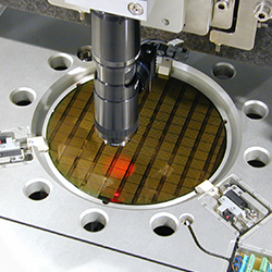
Various Kinds of Inspection are required in semiconductor industry production line: on-line inspection, critical dimension-measurement, and in-line inspection. Semiconductor Inspection System is the equipment used in manufacturing process of semiconductor device to detect the failure. Complete development of semiconductor device involves large manufacturing process. A failure at one step of the process, means to interrupt the subsequent step to avoid production of defective product. Hence insertion of inspection systems at the pivotal points of the process will ensure process moves to next step after confirming no defect at current step. Otherwise the production is interrupted if failure in the device is detected and the cause is determined followed by defect removal. Once the defect is sufficiently removed, the process is advanced to the next step in the process. Main defects in the semiconductor manufacturing process are pattern defects and small particles on semiconductor wafer. Semiconductor Inspection System detects both the pattern defects and physical defects (foreign substances like particles) by obtaining the coordinates(X, Y) of the defect’s position. Determining position (Coordinates) on the wafer is the primary role of the Semiconductor Inspection System. Inspection can be done on both patterned and bare wafer. Inspection systems for patterned and non-patterned wafer have different configurations. Based on configuration patterned inspection systems are categorized as bright field, electron beam, and dark field inspection systems. Non-patterned inspection system is used in equipment check by dummy wafers for cleanliness monitoring of the equipment. Physical Defects that are caused by foreign particle are called random defects as their position (i.e. coordinates) cannot be determined. On the other hand systematic defects are the defects which are result of exposure and conditions of the mask. They occur at the same position and hence are detectable by the inspection systems. These inspection systems are hence indispensable to maintain production yield of semiconductors.
Rise in demand for high performing and low cost semiconductors will augment the use of inspection systems. Growing complexity of the process and design of semiconductor chip is also significant factor in growth of the market for semiconductor inspection systems. Increasing demand for notebooks, gaming consoles, smartphones, tablets, network switches, digital cameras, and set-top boxes will propel the requirement of foundries. Increasing proliferation of loT (Internet of Things) is also the growth driver. Rising need of semiconductor memory devices like 3D NAND and DRAM is also attributed to growth of the market. The main challenge posed to the industry is introduction of multi-layer wiring and planarization process in manufacturing of semiconductor devices which existing inspection systems are incapable to detect.
Planning to lay down future strategy? Perfect your plan with our report sample here https://www.transparencymarketresearch.com/sample/sample.php?flag=S&rep_id=15788
The market can be segmented based on the type (wafer inspection system & mask inspection system), by technology (optical and e-beam), by end-users (memory manufacturer, IDMs, and foundries), and by geography. Wafer Inspection systems will continue to dominate the market. Also Foundries occupy the largest market share.
APAC is the major revenue-generating market for Semiconductor Inspection Systems. Increasing domestic IC production in this region is the key factor for growing demand in this market. India, Nepal, Bangladesh, and Thailand are the major markets in APAC. However North America has the largest market for the Semiconductor Inspection Systems followed by U.S. and Canada. The second largest market for Semiconductor Inspection Systems is APAC. Europe has seen a moderate growth in terms of Semiconductor Inspection Systems. Germany, being the largest electronics manufacturer and automotive hub, contributes immensely to the Semiconductor Inspection Systems in Europe market. Strong acquisitions and mergers strategies by semiconductor vendors will drive growth in the Europe market.
Key players in the Semiconductor Inspection Systems market are KLA-Tencor, Applied Materials, Hermes Microvision, and Lasertech. Other vendors include ASML Holding, JEOL, Carl Zeiss, Hitachi High-Technologies, Nikon, Nanometrics, Lam Research, Planar Corporation, Rudolph Technologies, Toray Engineering, and Tokyo Seimitsu.
The report offers a comprehensive evaluation of the market. It does so via in-depth qualitative insights, historical data, and verifiable projections about market size. The projections featured in the report have been derived using proven research methodologies and assumptions. By doing so, the research report serves as a repository of analysis and information for every facet of the market, including but not limited to: Regional markets, technology, types, and applications.
Looking for exclusive market insights from business experts? Buy Now Report here https://www.transparencymarketresearch.com/checkout.php?rep_id=15788<ype=S
The study is a source of reliable data on:
- Market segments and sub-segments
- Market trends and dynamics
- Supply and demand
- Market size
- Current trends/opportunities/challenges
- Competitive landscape
- Technological breakthroughs
- Value chain and stakeholder analysis
The regional analysis covers:
- North America (U.S. and Canada)
- Latin America (Mexico, Brazil, Peru, Chile, and others)
- Western Europe (Germany, U.K., France, Spain, Italy, Nordic countries, Belgium, Netherlands, and Luxembourg)
- Eastern Europe (Poland and Russia)
- Asia Pacific (China, India, Japan, ASEAN, Australia, and New Zealand)
- Middle East and Africa (GCC, Southern Africa, and North Africa)
The report has been compiled through extensive primary research (through interviews, surveys, and observations of seasoned analysts) and secondary research (which entails reputable paid sources, trade journals, and industry body databases). The report also features a complete qualitative and quantitative assessment by analyzing data gathered from industry analysts and market participants across key points in the industry’s value chain.
A separate analysis of prevailing trends in the parent market, macro- and micro-economic indicators, and regulations and mandates is included under the purview of the study. By doing so, the report projects the attractiveness of each major segment over the forecast period.
Highlights of the report:
- A complete backdrop analysis, which includes an assessment of the parent market
- Important changes in market dynamics
- Market segmentation up to the second or third level
- Historical, current, and projected size of the market from the standpoint of both value and volume
- Reporting and evaluation of recent industry developments
- Market shares and strategies of key players
- Emerging niche segments and regional markets
- An objective assessment of the trajectory of the market
- Recommendations to companies for strengthening their foothold in the market
Note: Although care has been taken to maintain the highest levels of accuracy in TMR’s reports, recent market/vendor-specific changes may take time to reflect in the analysis.
This study by TMR is all-encompassing framework of the dynamics of the market. It mainly comprises critical assessment of consumers’ or customers’ journeys, current and emerging avenues, and strategic framework to enable CXOs take effective decisions.


